
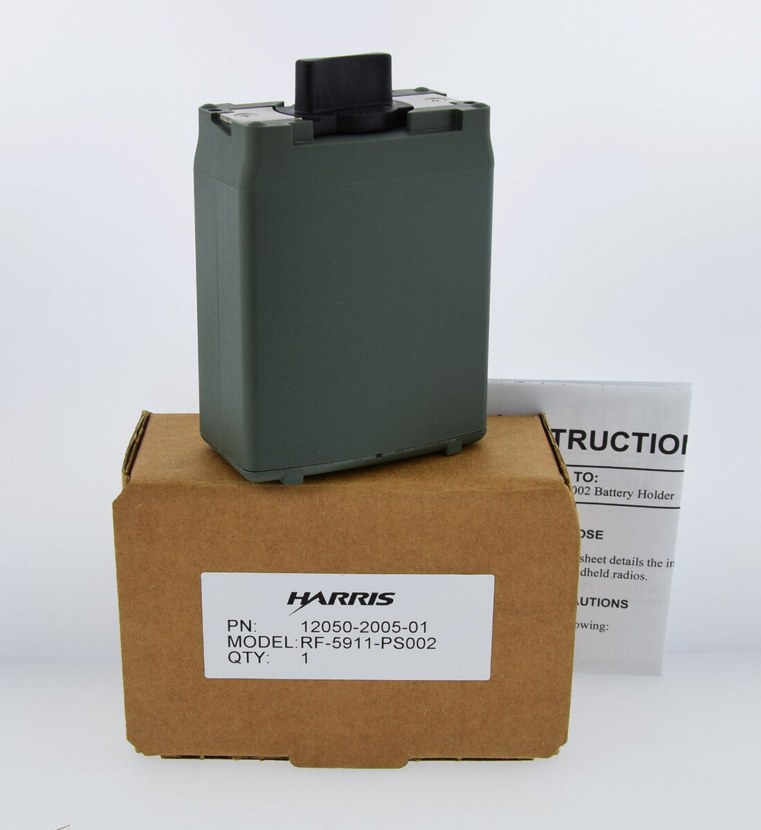
Teardown: Harris 12050-2005-01, RF-5911-PS002, L123 Battery Holder
Last Update: November 30th, 2024
Table of Contents
Introduction
Generic image "borrowed" from eBay.
A Duracell CR123 costs about five bucks each, so a full case would cost you fifty bucks. Occasionally my interests and hobbies line up. In this case: Radios? Check. Militaria? Check. Batteries? Check. (Not necessarily in that order.) Harris equipment tends to command a premium on the usual auctions site (for good reason), but recently I stumbled across somebody liquidating a stock of these battery cases for a somewhat reasonable price. For various reasons I have an interest in proving out the "pin out" of this de facto form factor, so I grabbed an example for the sole purpose of tearing it apart. What I thought might prove maybe an hour of amusement and a simple "beeping out" of the circuit with a multimeter, turned out to be surprisingly complex and involved, and the design even includes a small mystery. The usual disclaimers apply here: This is not a repair or rebuild guide. This is a one-way operation - this case will never operate correctly again. Follow along at your own risk.
Teardown Photos
As one would expect from expensive, military-oriented hardware, the build quality of the case is excellent. On close examination it's obviously plastic, but it feels surprisingly cold and metallic to the touch - I wonder what filler they used.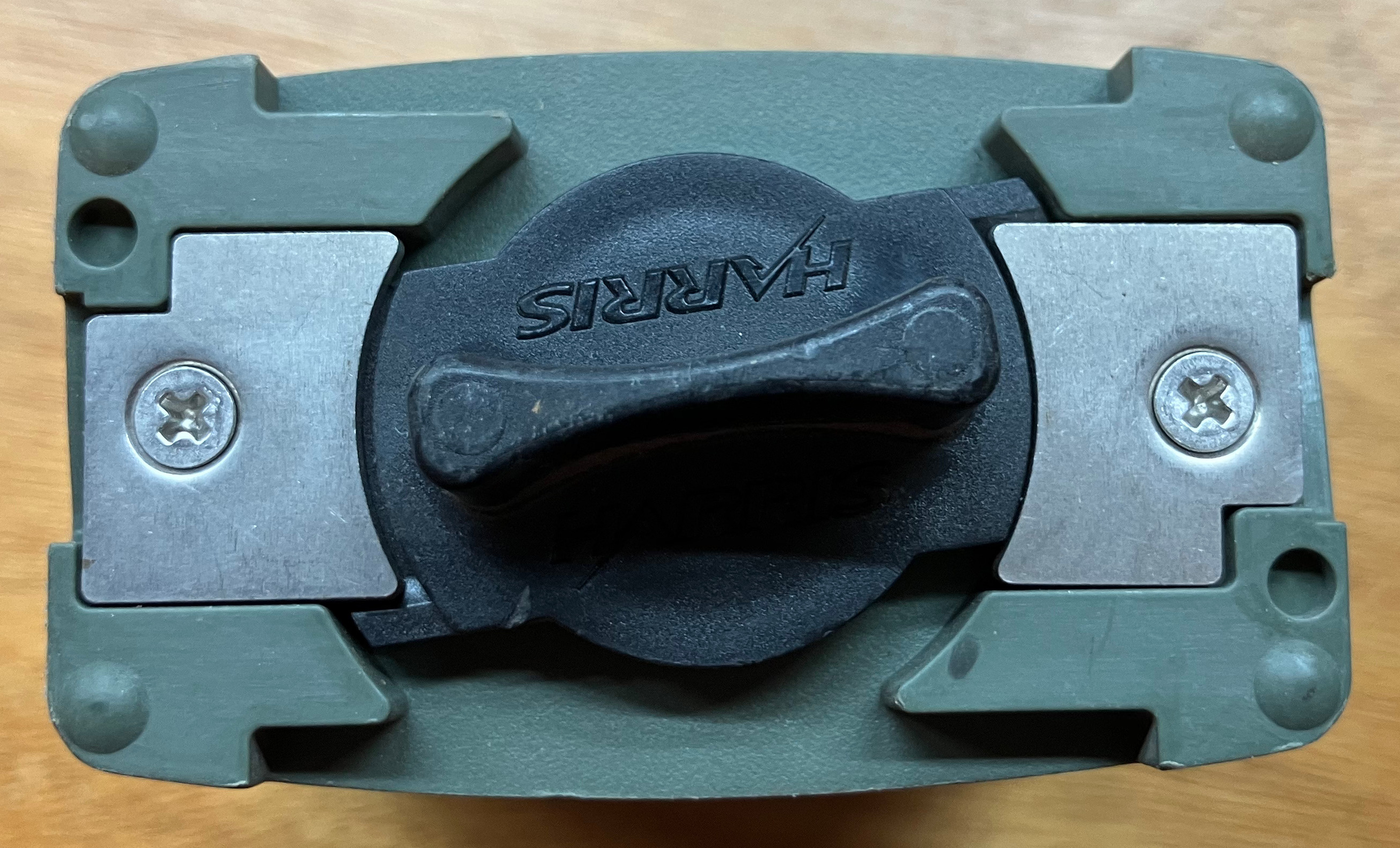
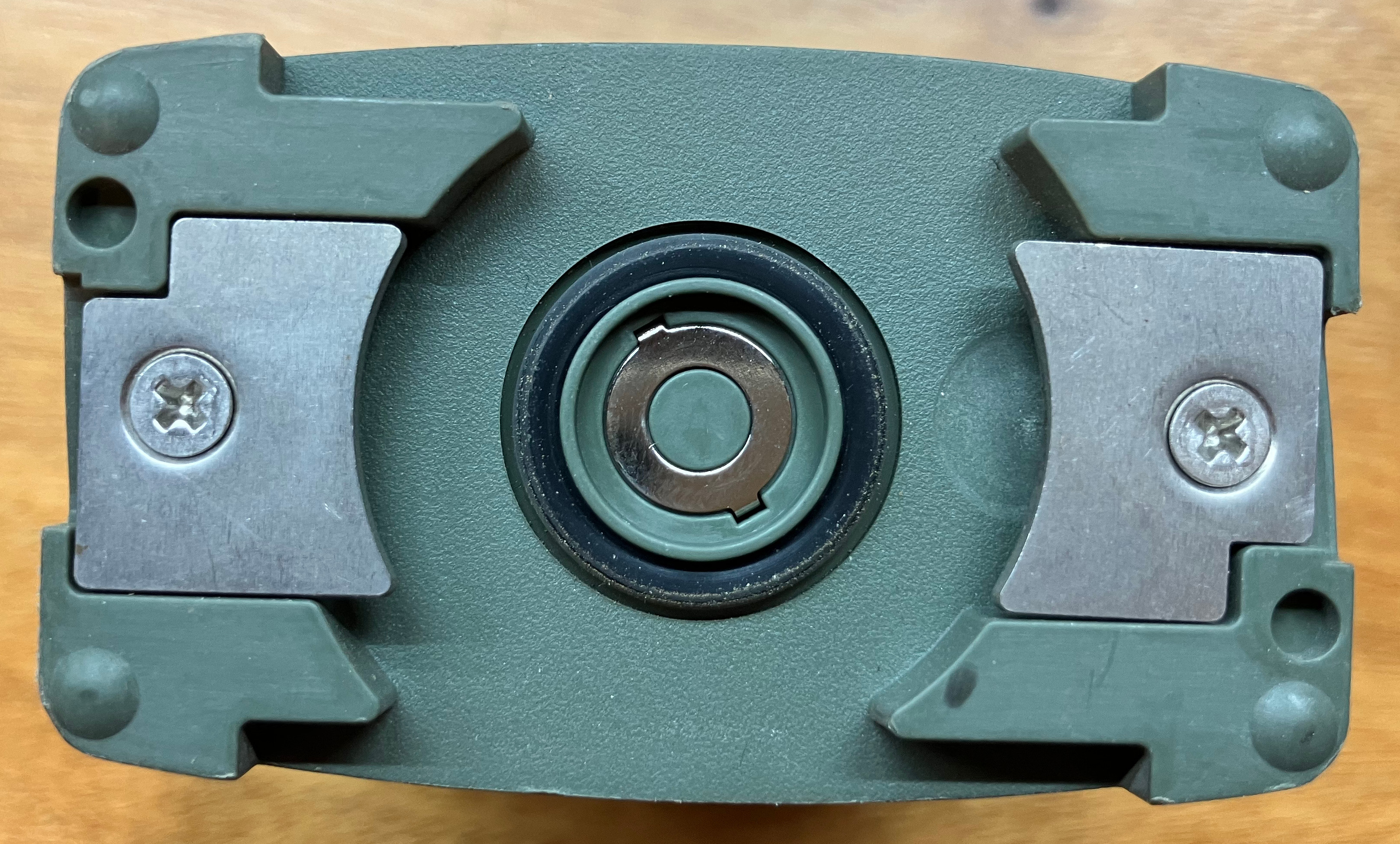
Exterior of the case.
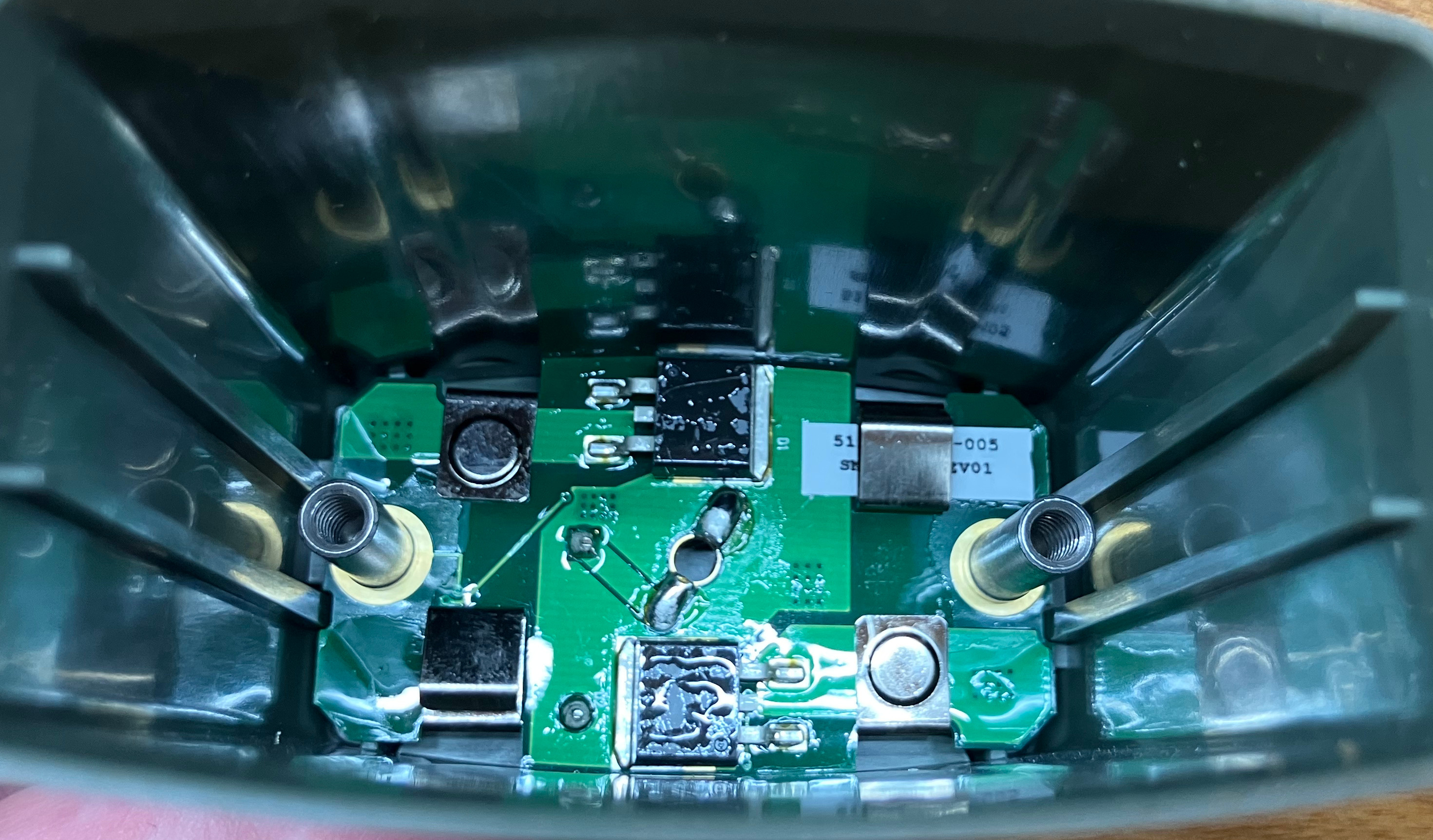
Inside, looking up.
Just grab the standoffs with a pair of grippy pliers and use a Phillips. You'll need some force to crack the weather sealant.
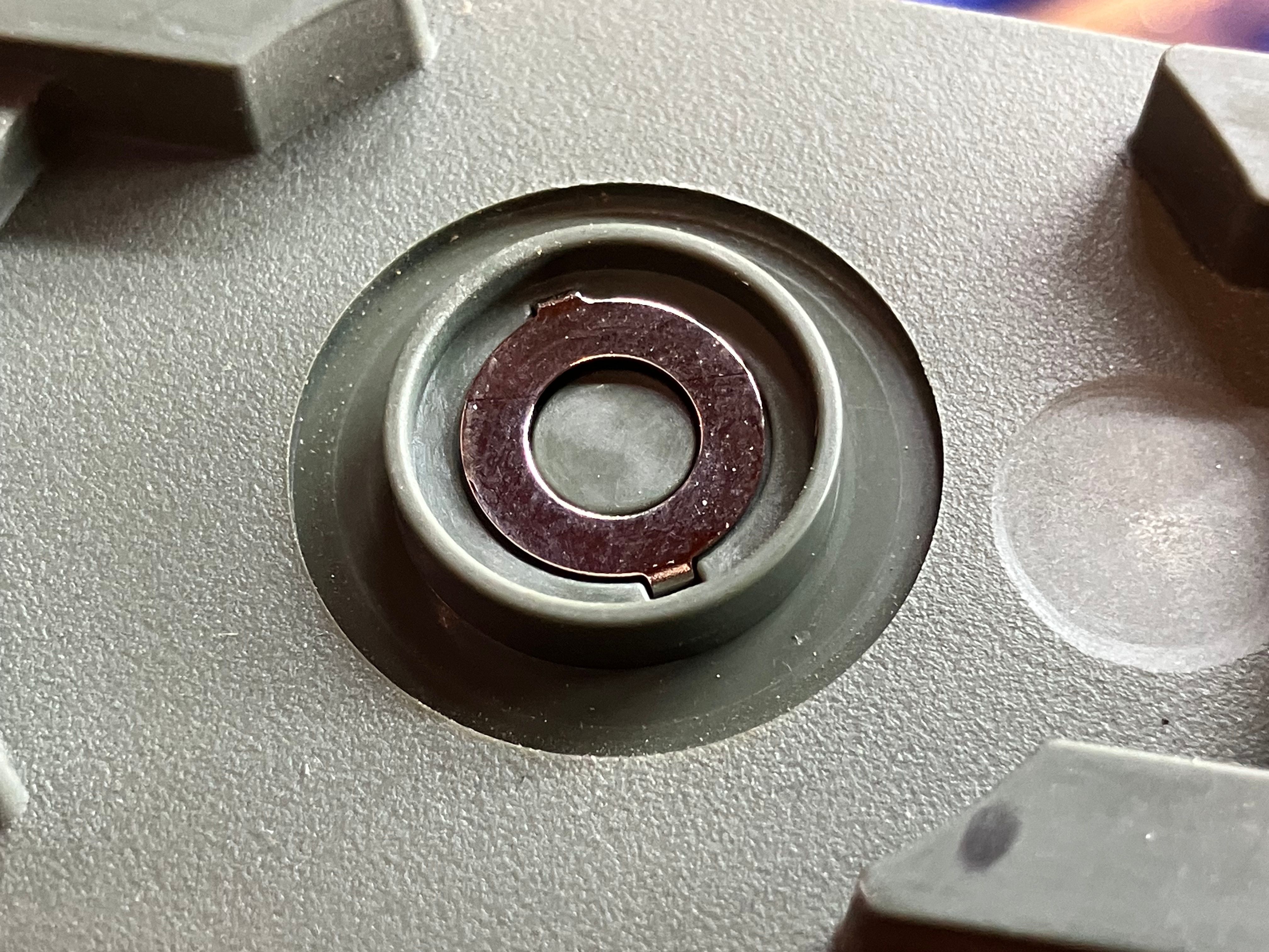
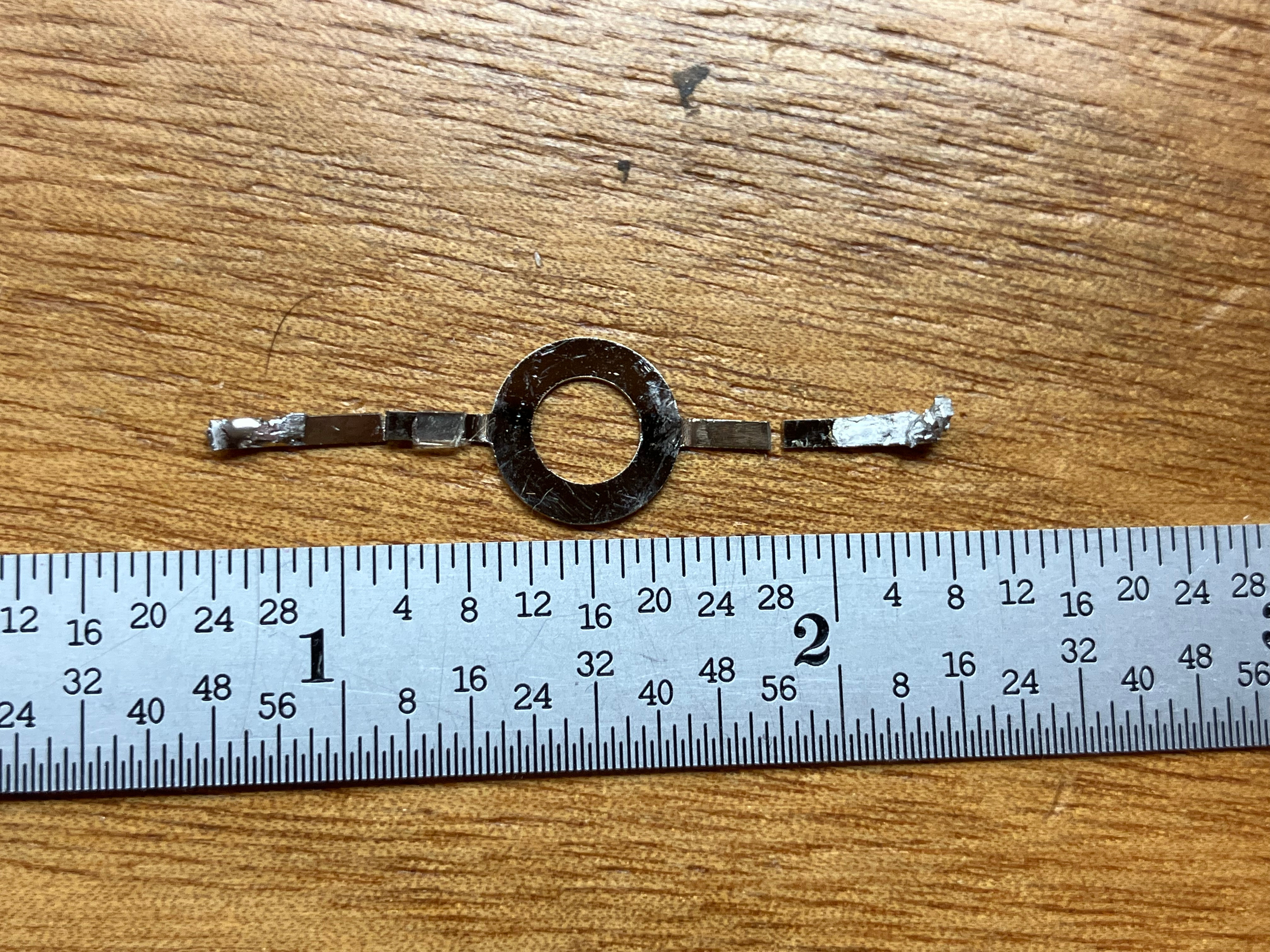
Contact Ring popping out.
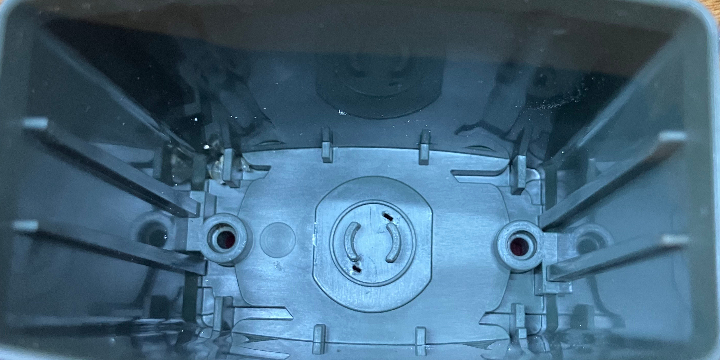
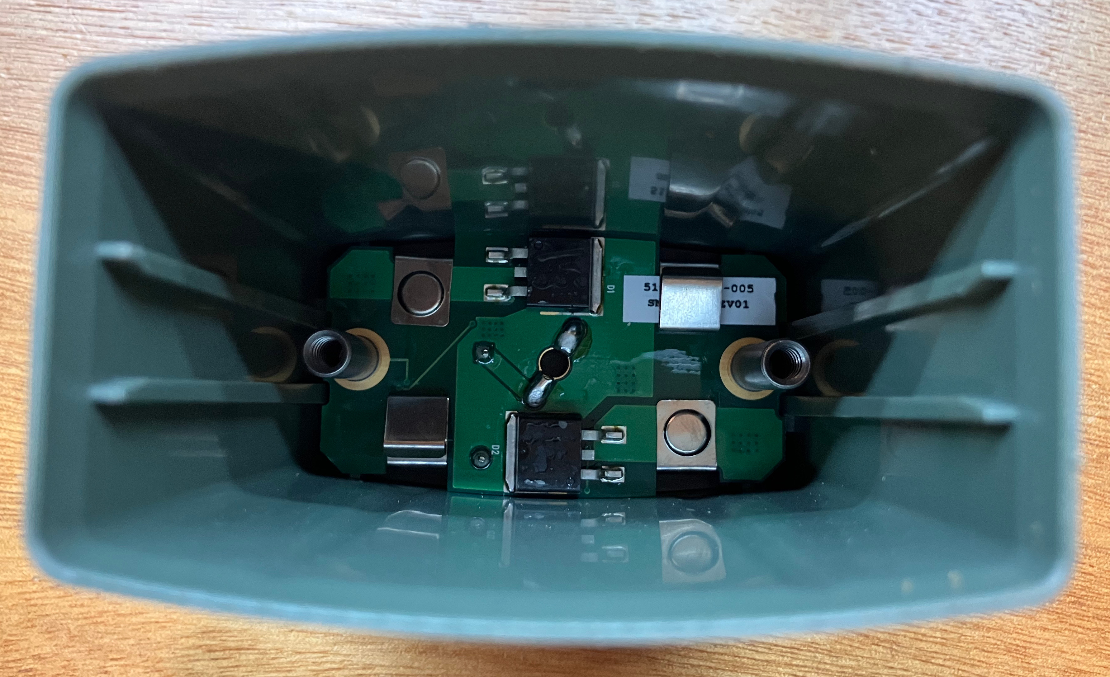
Detail of the interior molding.
Note the ejection pin spot on the left side.
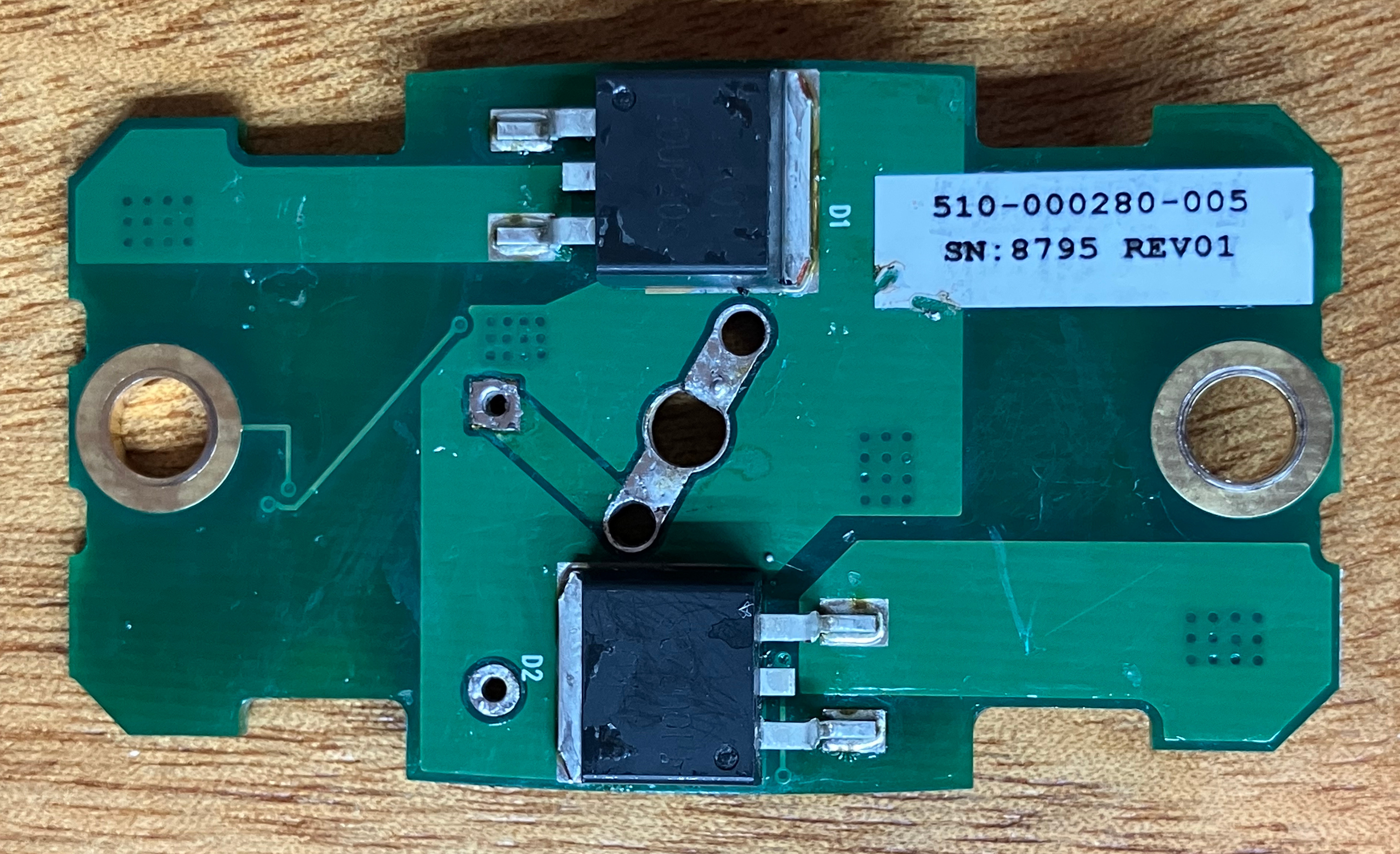
First look
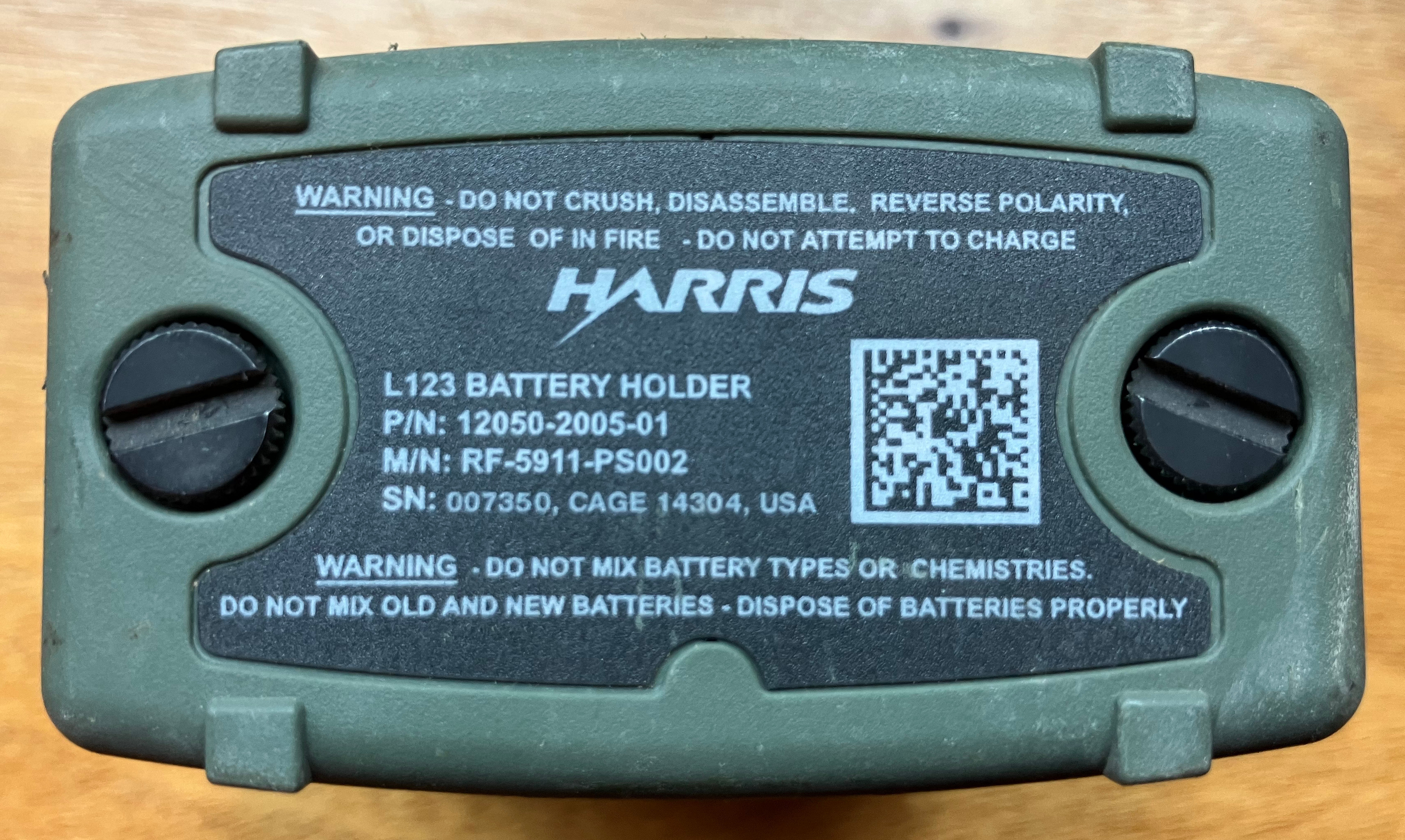
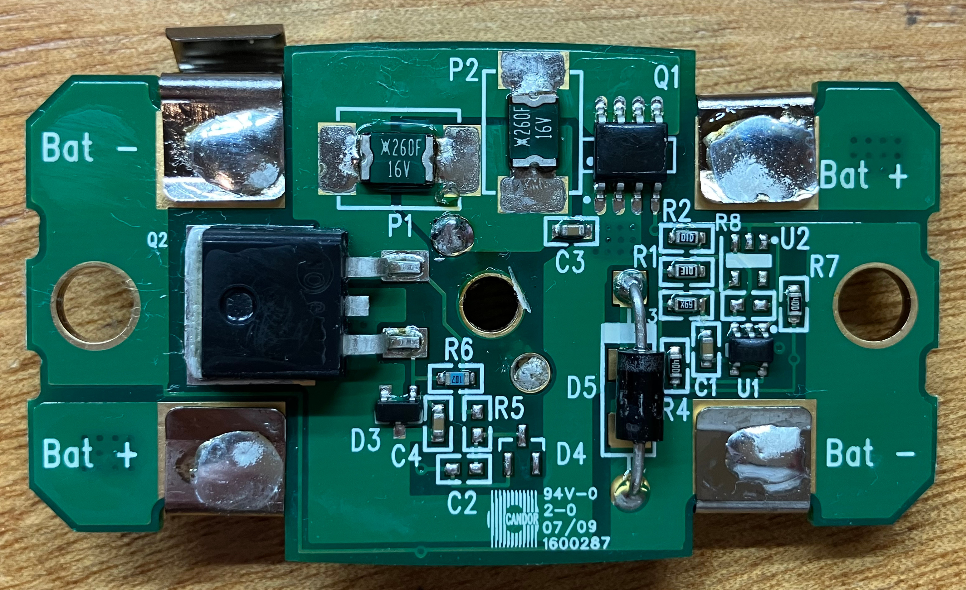
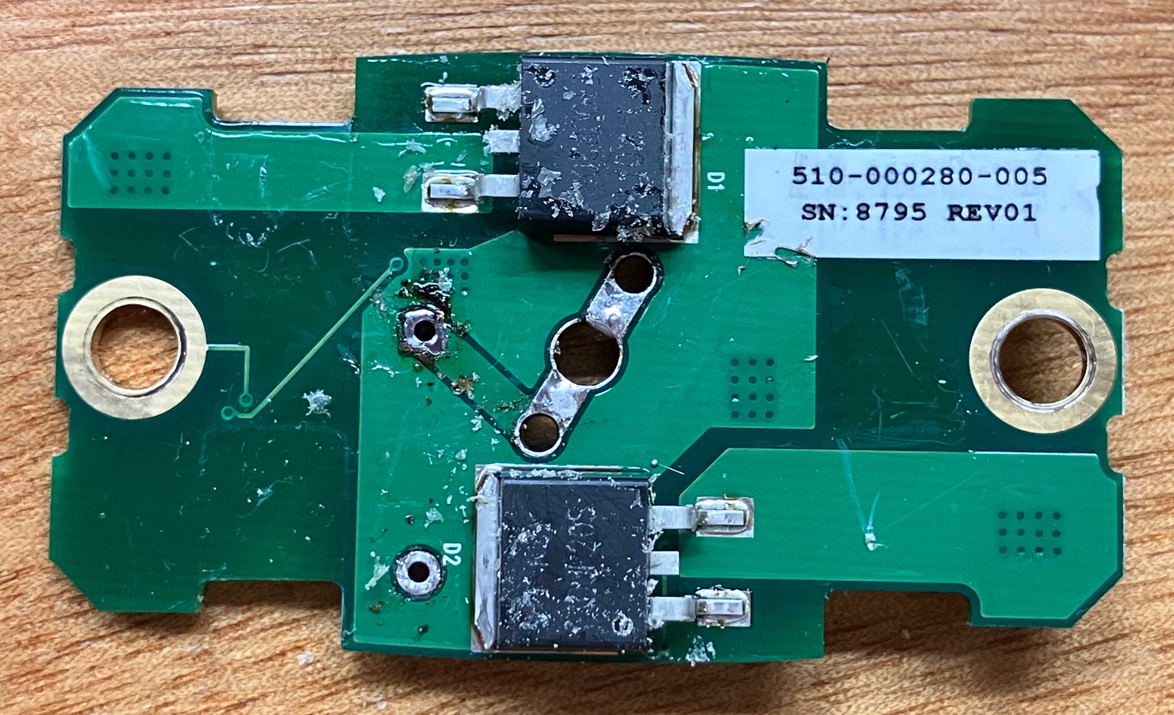
	CANDOR (logo)
	94V-0
	2-0
	07/09
	1600287

	510-000280-005
	SN: 8795 REV01
Presumably the PCB was manufactured in July of 2009, making this case around 16 years old.
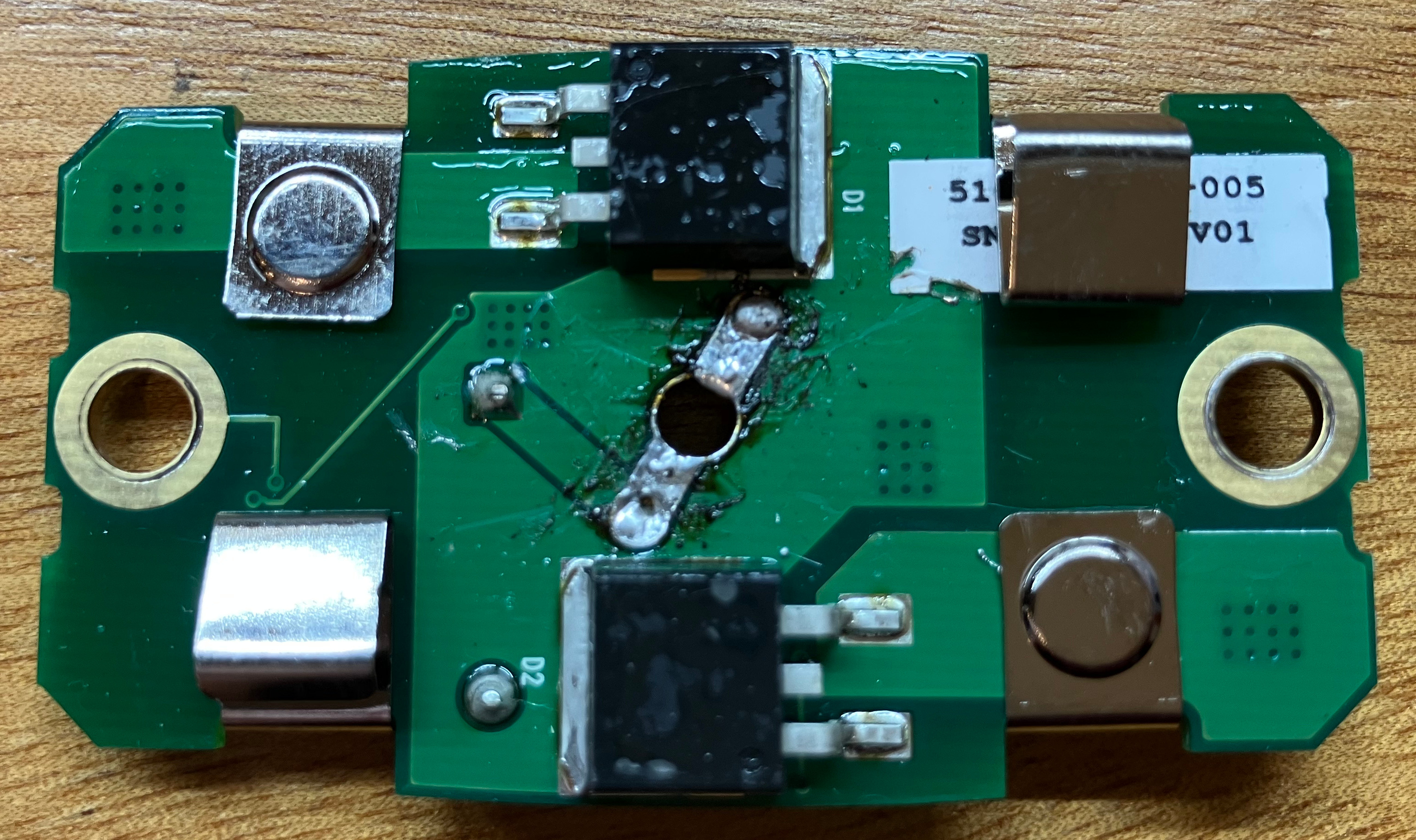
Conformal coating, detail
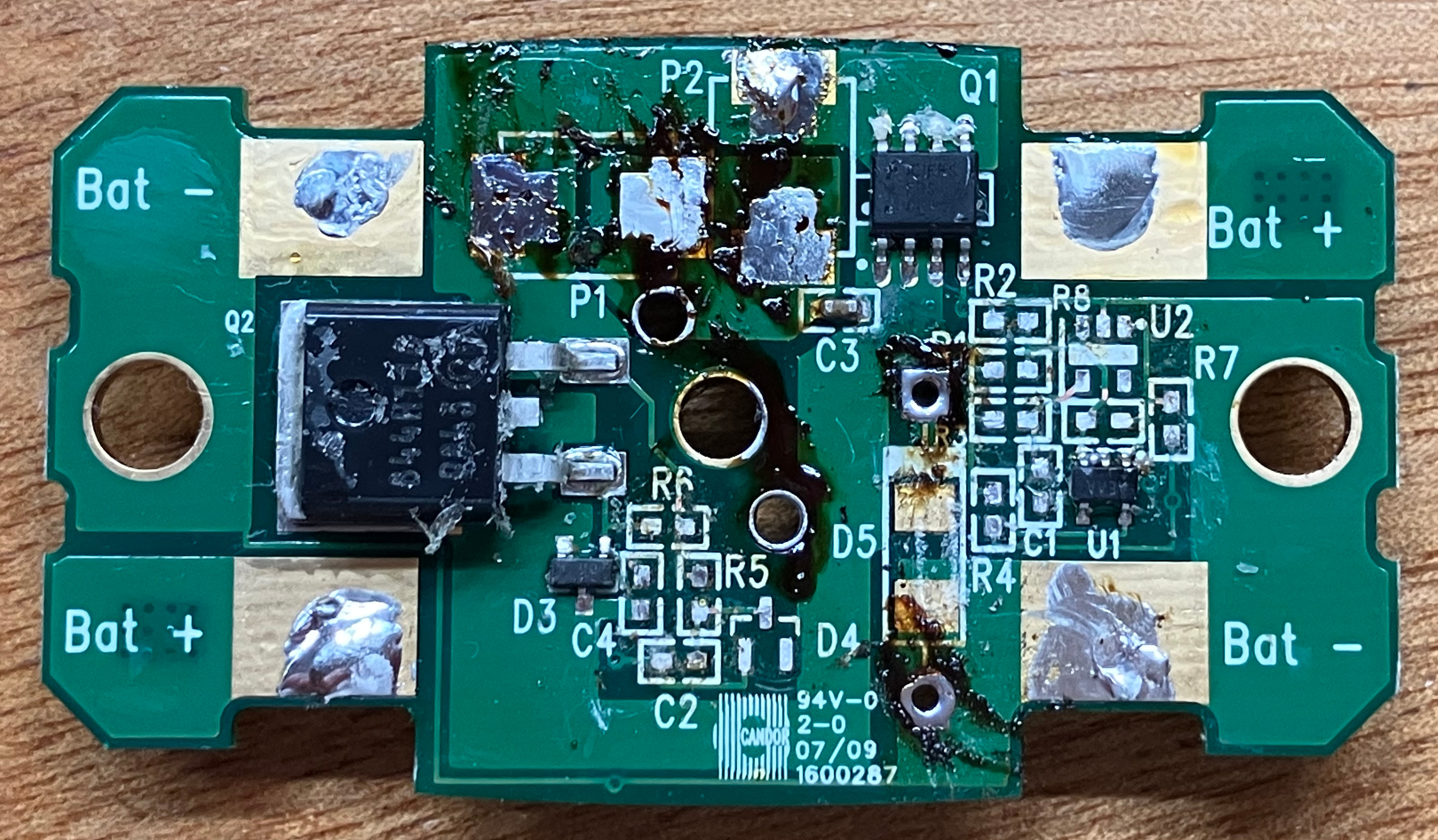
Parts and coating removed
That's a new one for me. I was expecting to have to mop up hot-melt or something. I waved my hot air rework gun over the parts and the coating started cracking. Some careful work with a knife blade scraped it right off. I went at a lot of the parts with a chunky soldering iron and just plowed them right off the board, and then went over all the pads solder braid to wick up excess material. Also took off the battery clips. Pro tip: Forget the IPA for board cleaning. I've found it's really not that effective. Acetone, q-tips, and a little bit of scrubbing are your friends. That got all the flux-gunk off this board. After that, I hit it with some 409 and an old toothbrush, which cleaned off everything else, and presumably removed all the now-loose conformal coating. Just don't forget to capture that waste stream, evap the fluids, and then package the residue for HAZMAT/solder debris disposal.
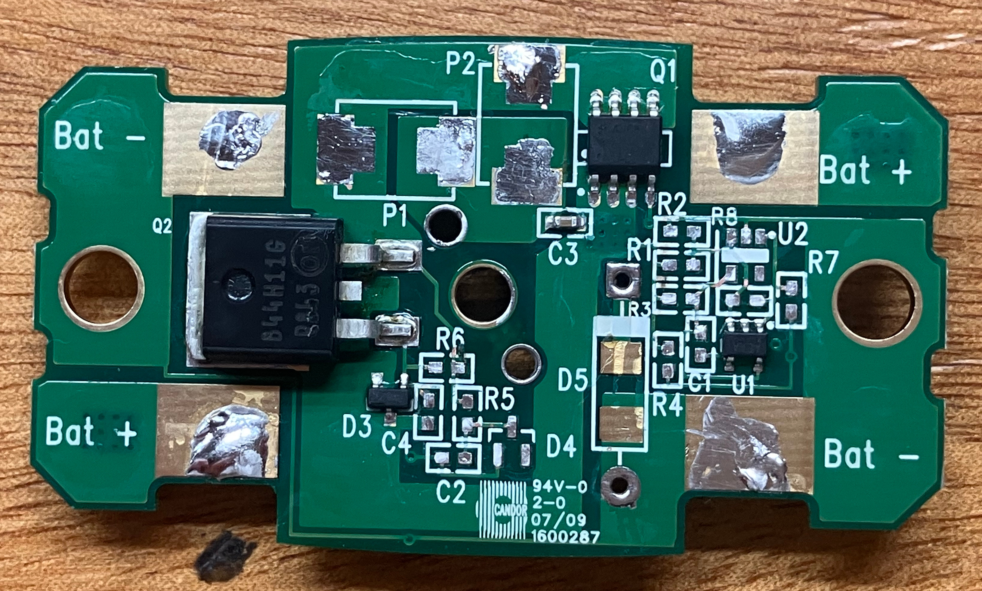
Cleaned Up
Theory of Operation
I highly recommend following along on the schematic, linked in the next section. A lot of the note here are going to be mirrored in the schematic as well.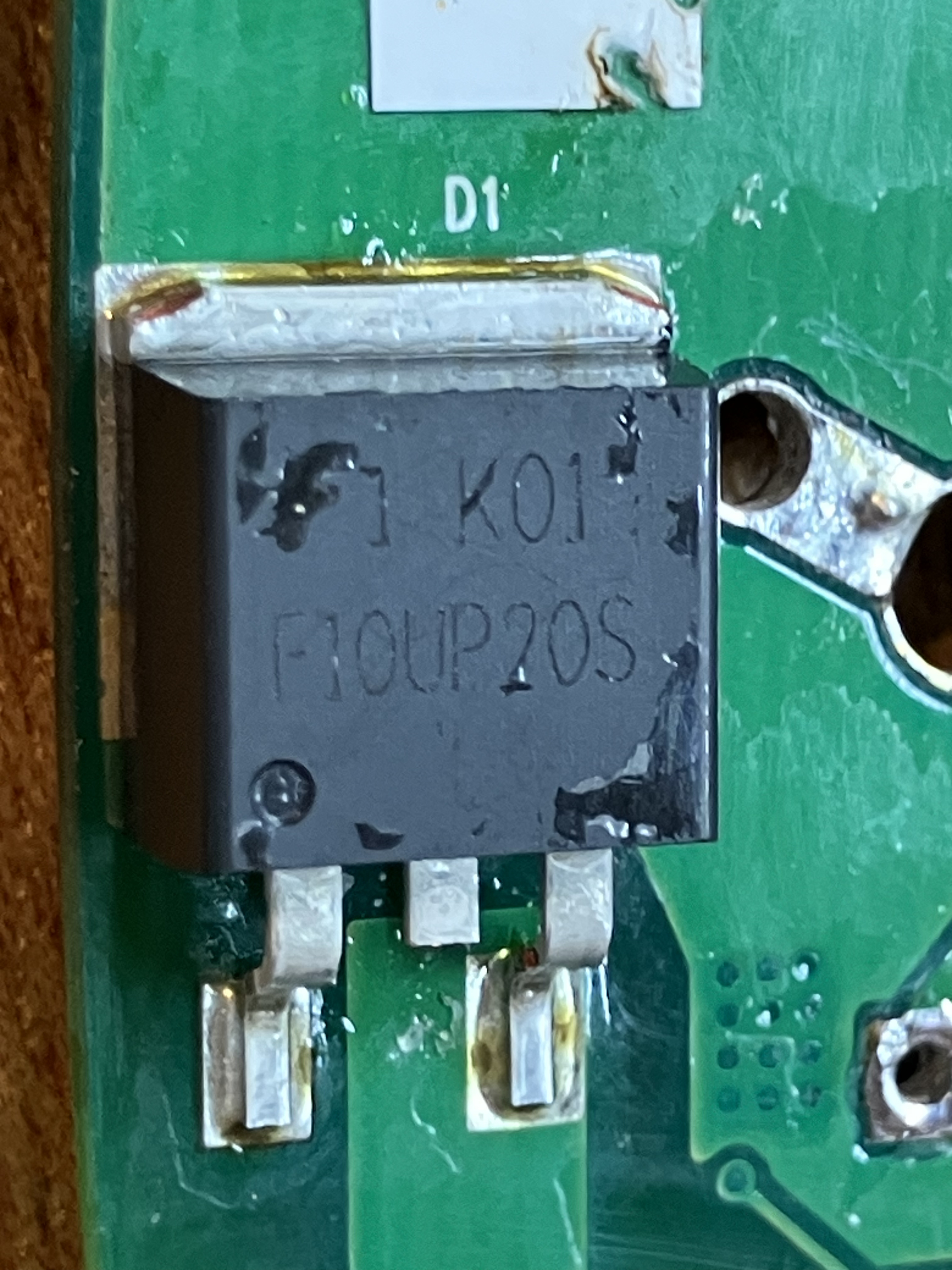
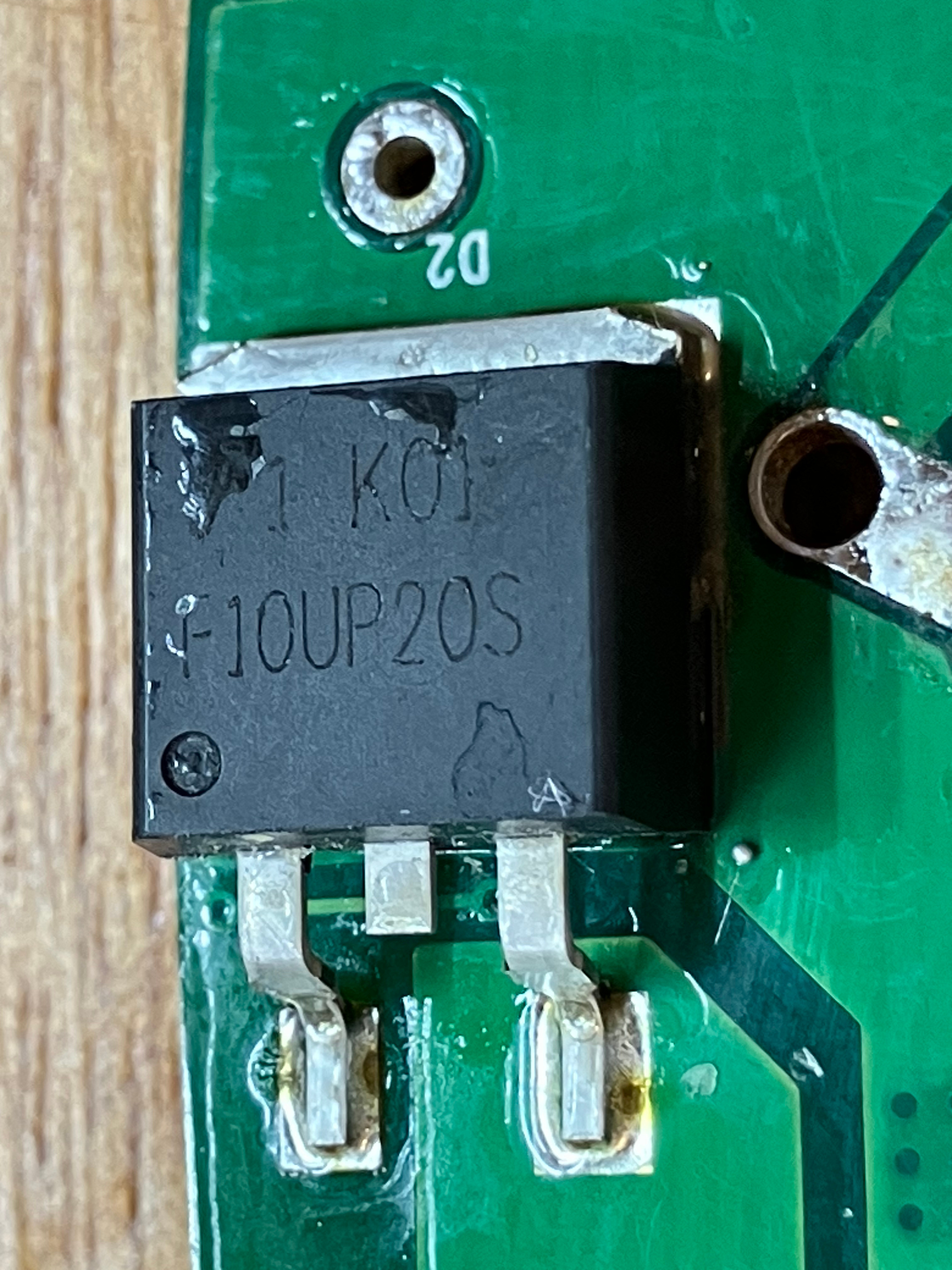
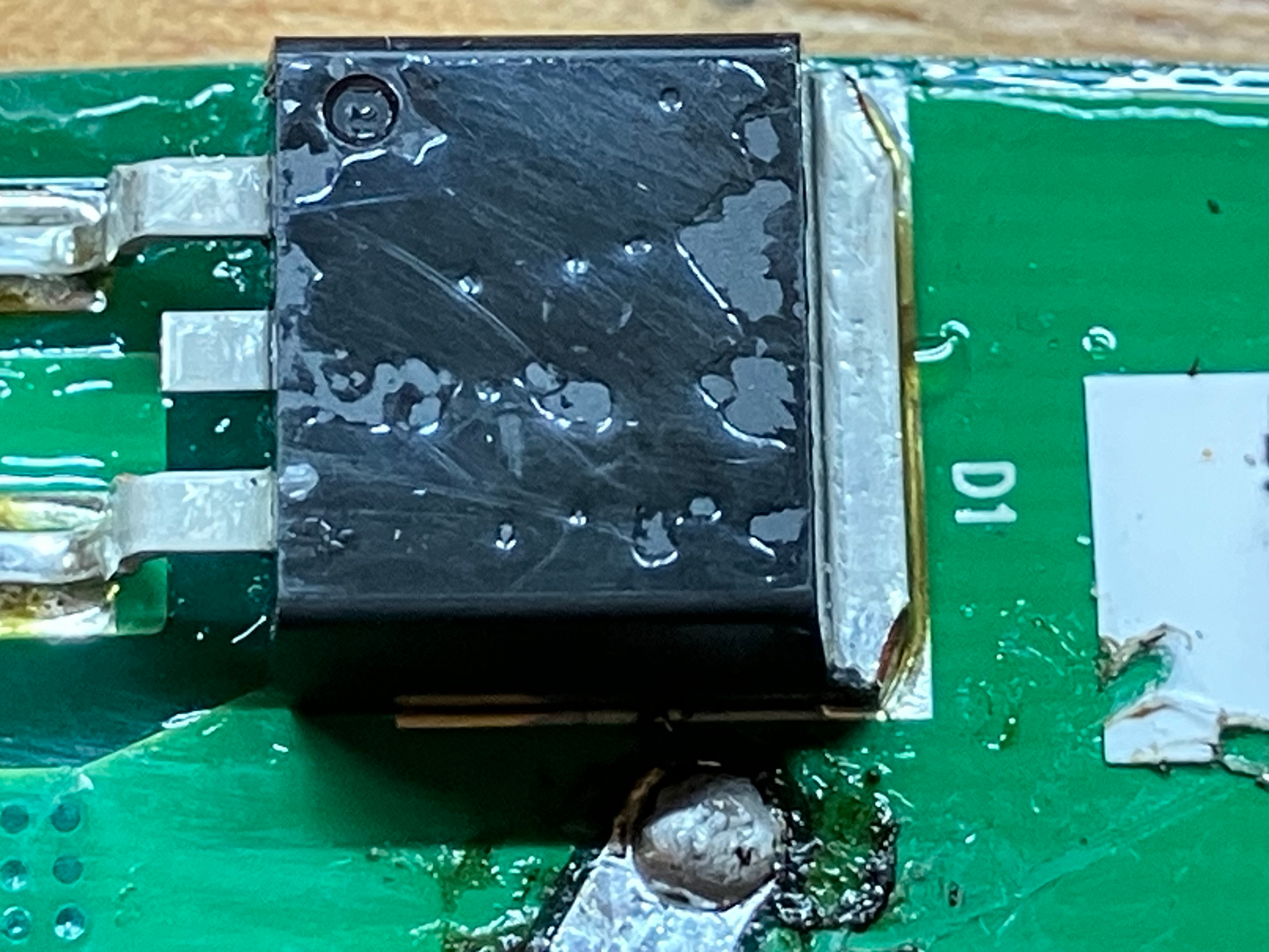
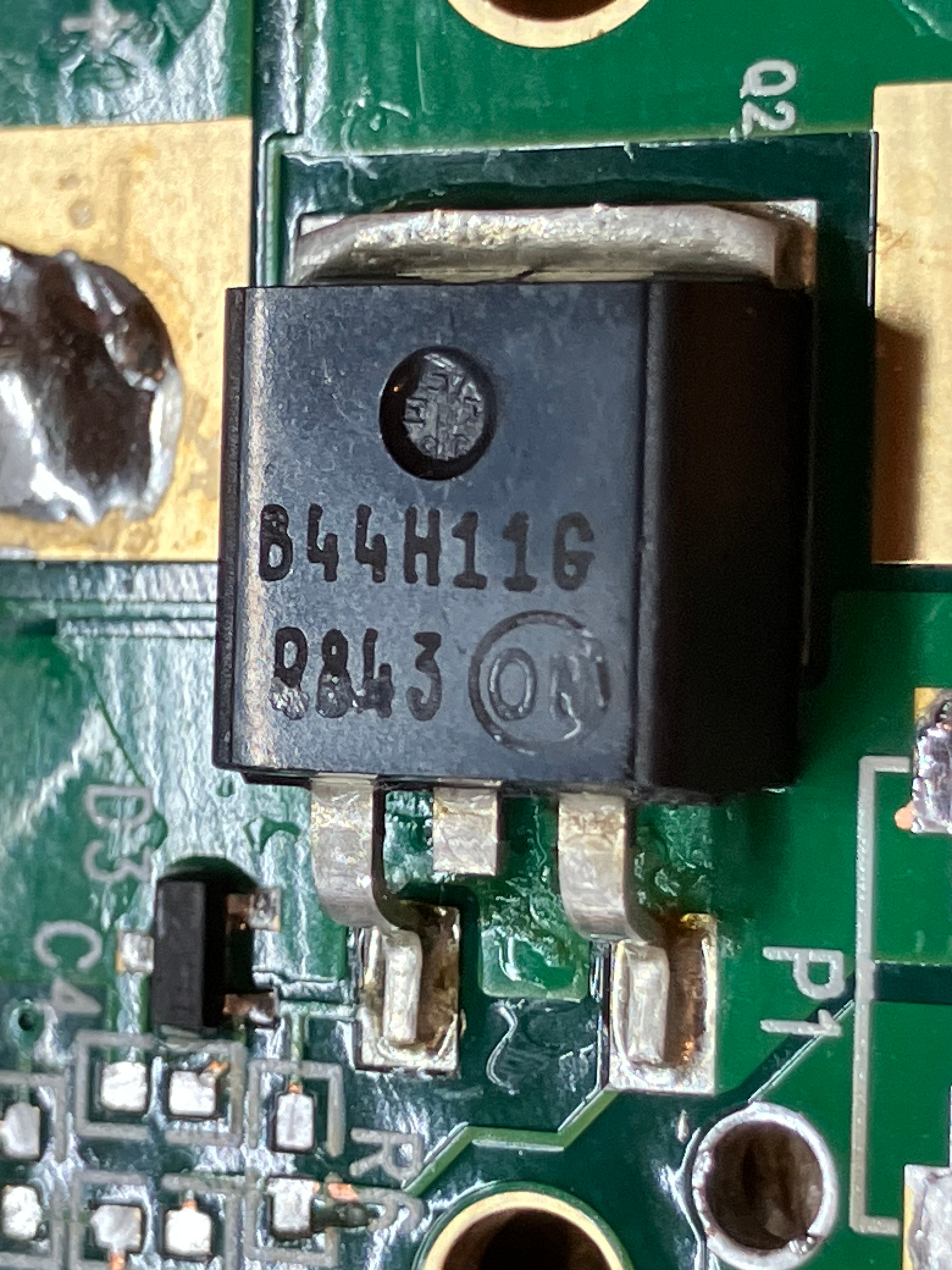
Power Diodes
Figure three in the official datasheet puts the Forward Voltage as a range from 0.5 V to 1.15 V.
A current draw as little as one amp - not exactly "out of sight" for a portable military radio - puts 500 mA across each diode. The VF for 500 mA works out to about 0.55 V - each diode would be dissipating about 0.27 W each.
In otherwords, during normal operation, the system would be wasting over half a Watt of battery energy as pure heat, before it even gets into the radio! Assuming a typical CR123 has 1400 mAh of energy, a full pack in this case would provide 41 Wh of energy. Adding half a Watt to your operation draw isn't the end of the world, but is def substantial. This seems like a tremendous waste. Granted this was designed 16 years ago, so these parts may have hit unknown-to-me price point and availability goals for the project. Semiconductors aren't free.
Nowadays, we certainly have parts that are better than this. (If anybody has any comments on this, maybe something I missed or did incorrectly, please shoot me an email.)
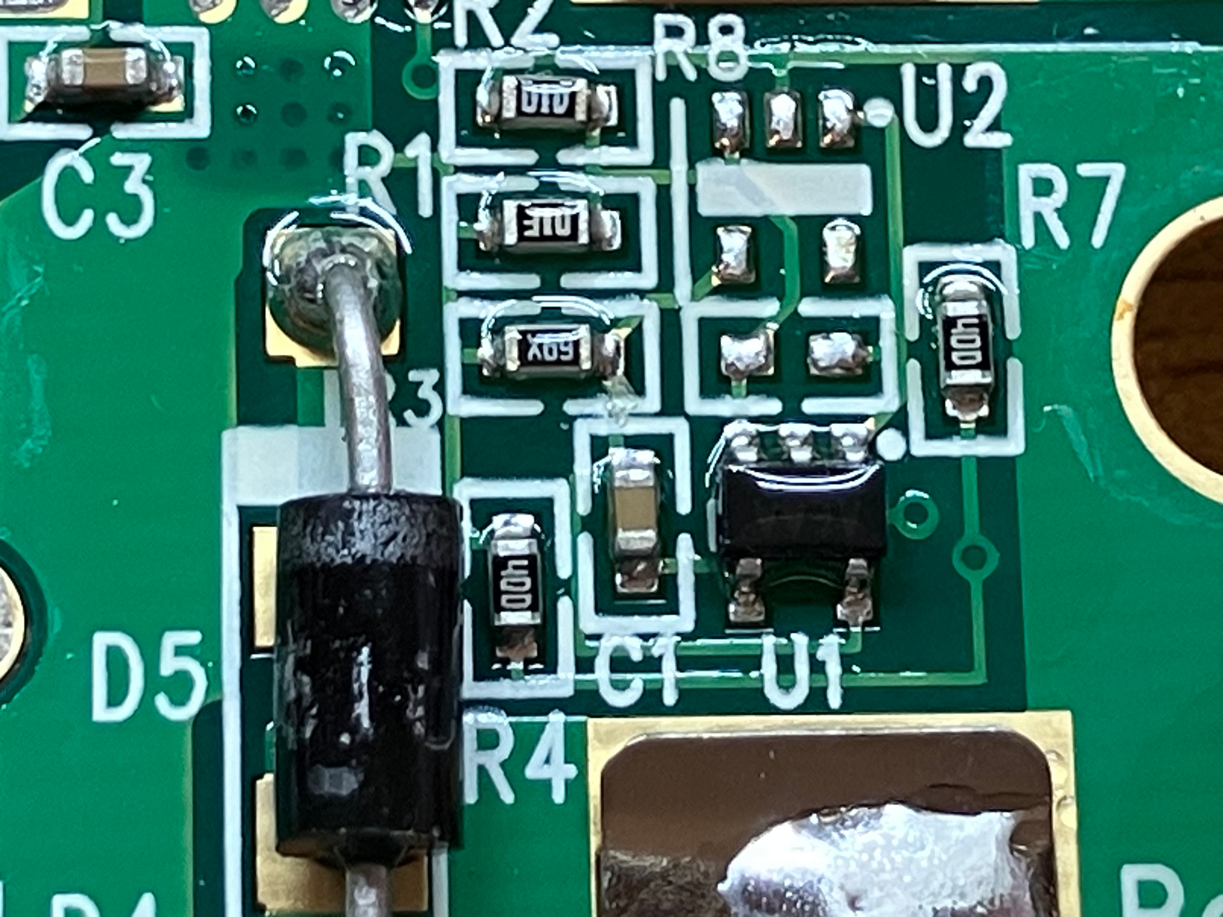
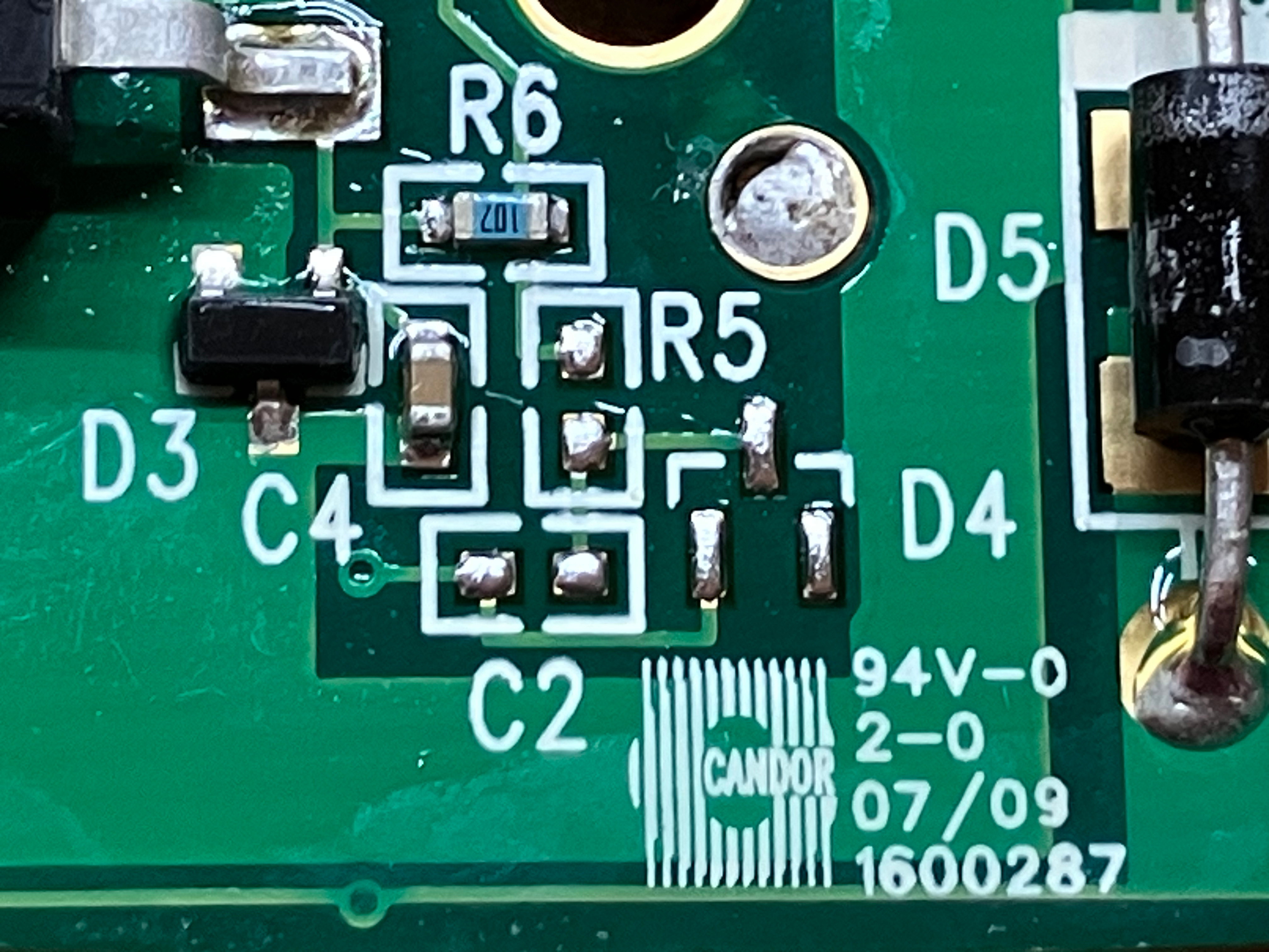
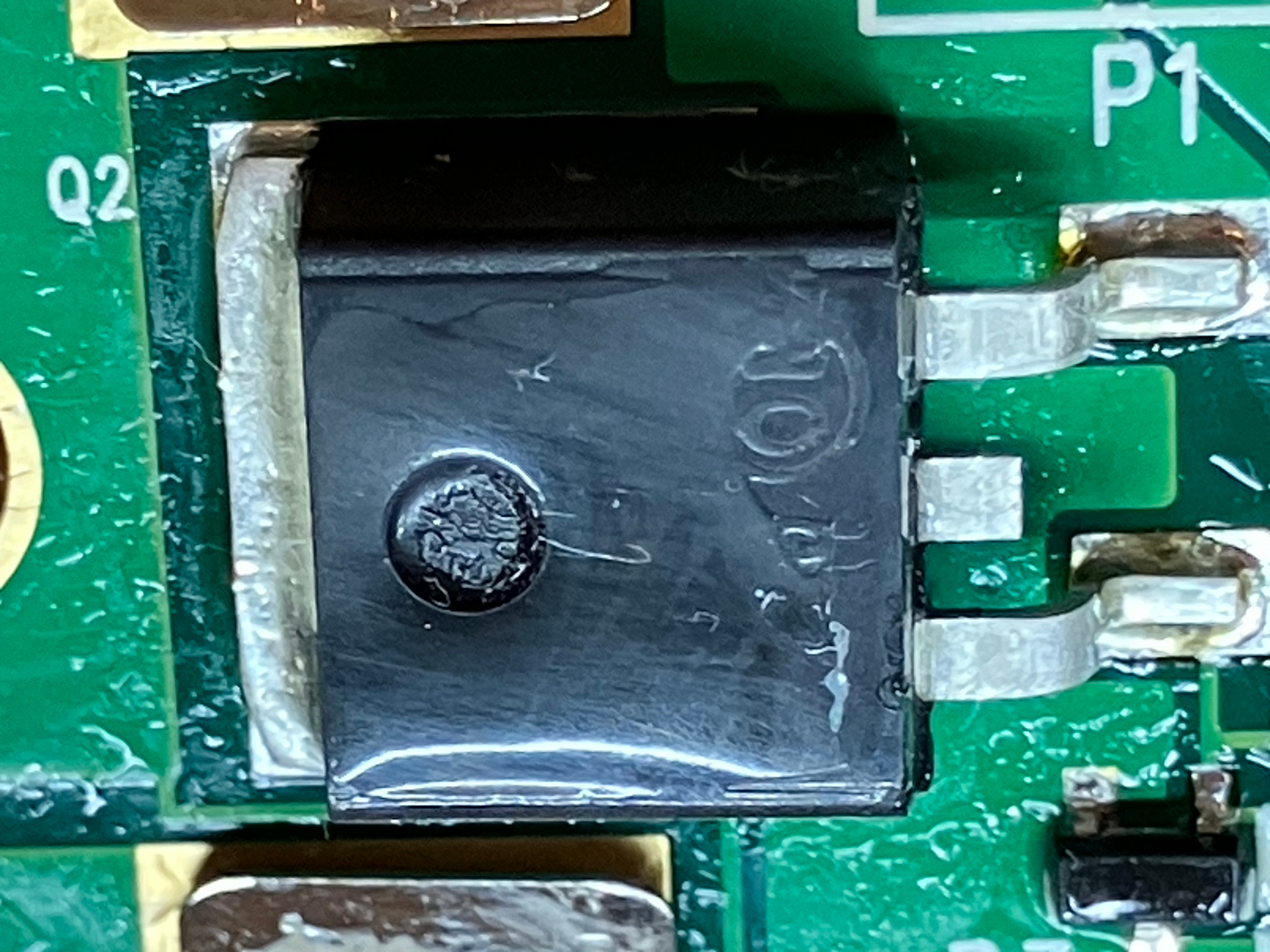
Q1/U1 complex, left. Q2 complex, right.
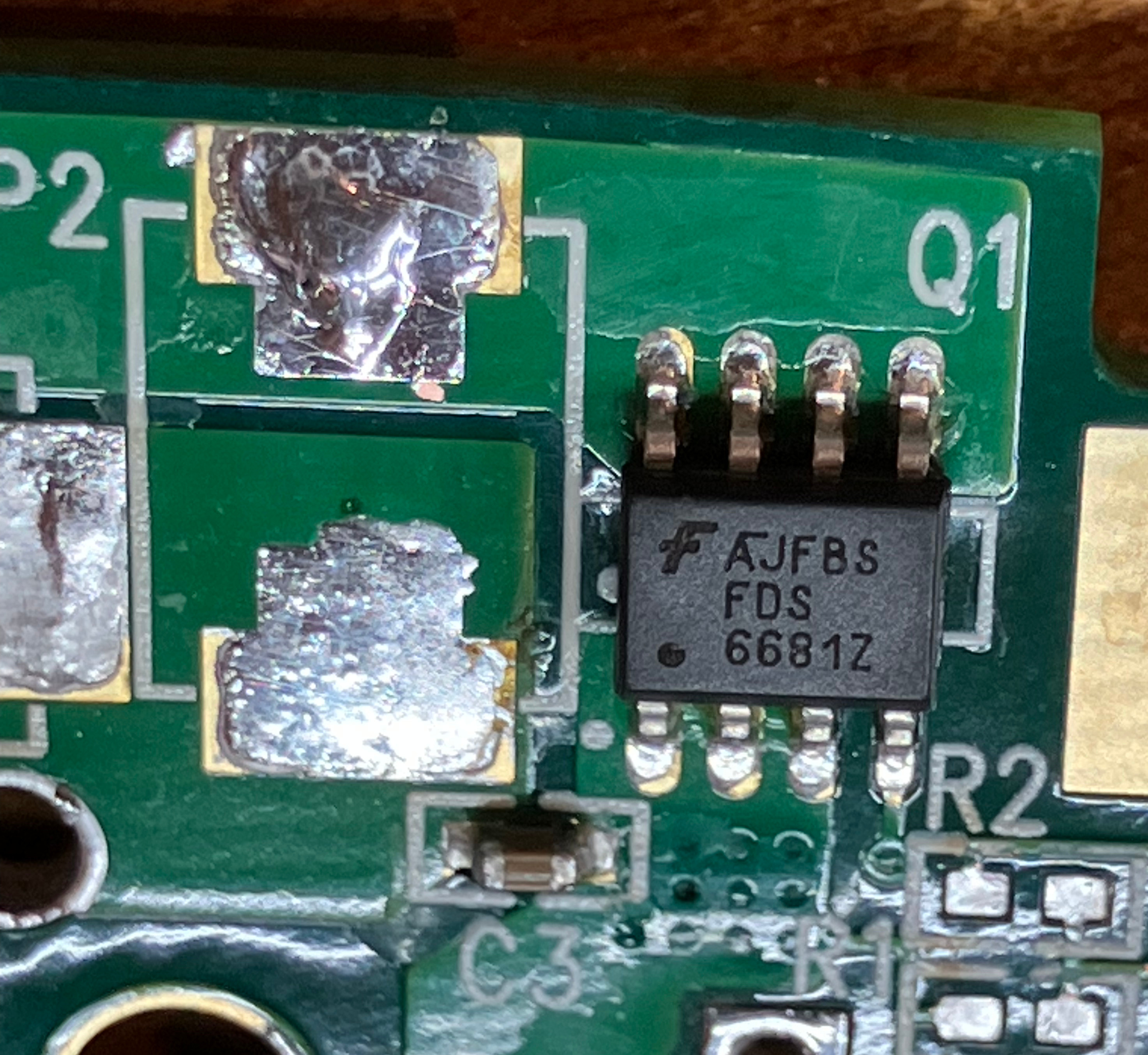
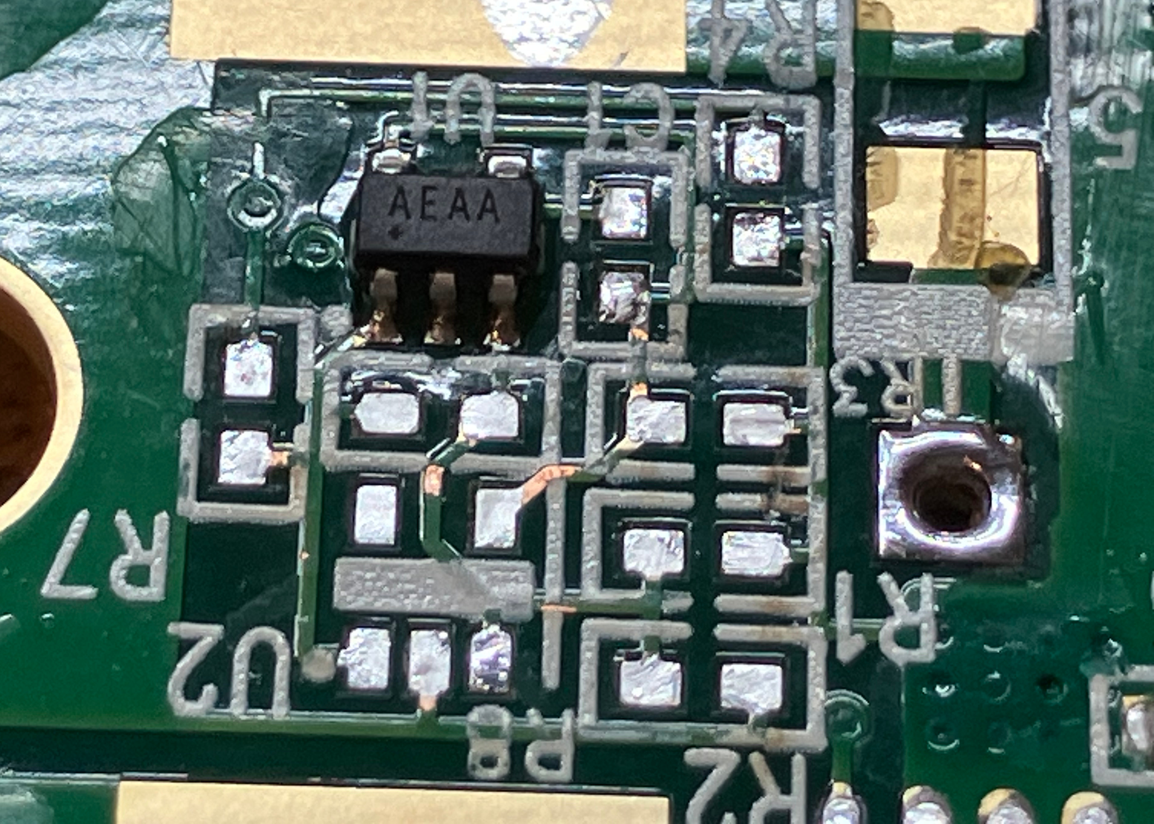
Q1/U1 Complex
In otherwords, if the output voltage of the cell strings drop too low, U1 senses this and opens the high side power switch (Q1). This is kind of interesting as I would have expected the radio to have a certain amount of functionality in regards to low battery detection, and make the final decision when to switch off. Maybe some radios this battery could connect to don't have that, or they just want to Be Really Sure nothing would brown-out.
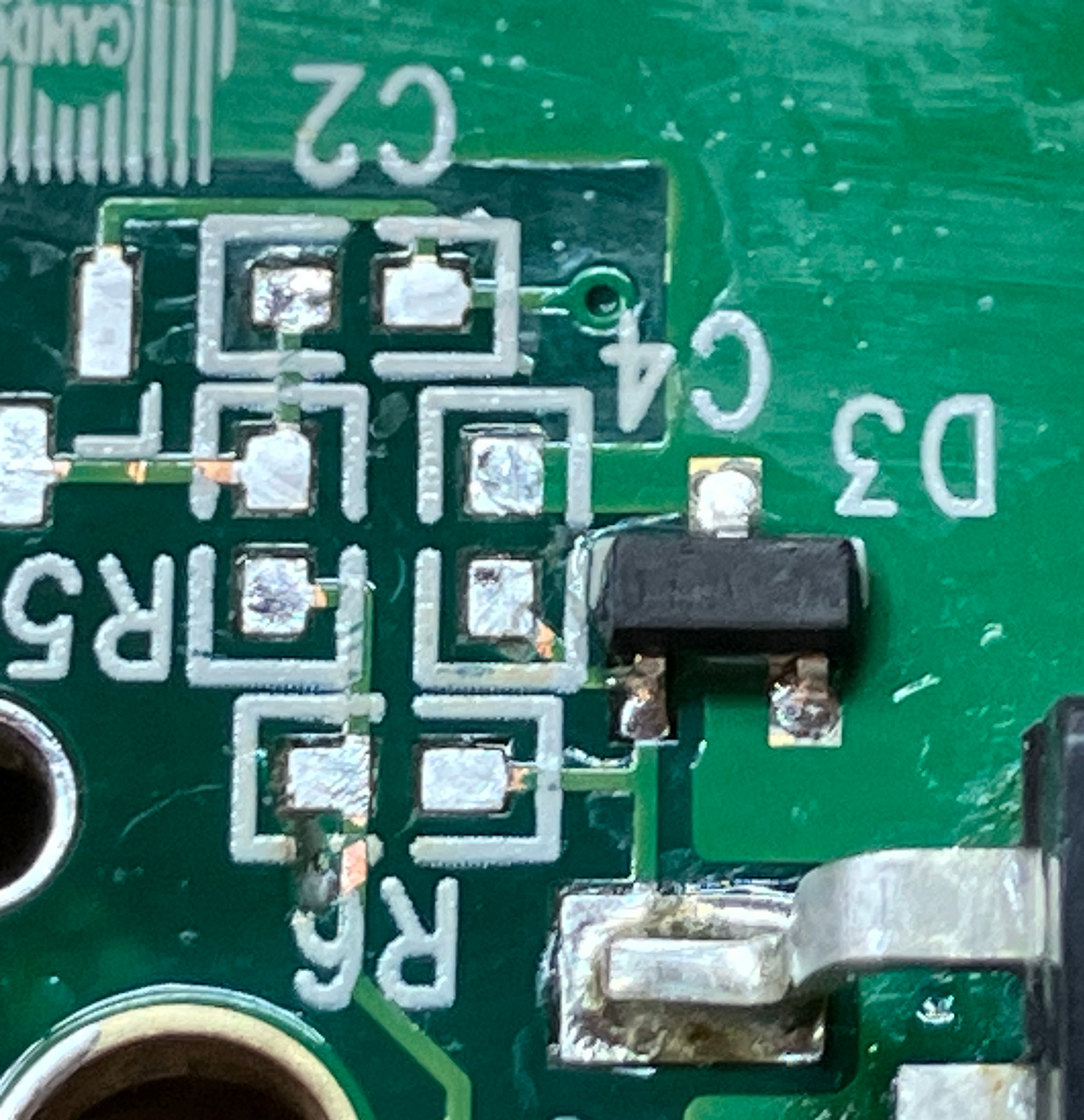
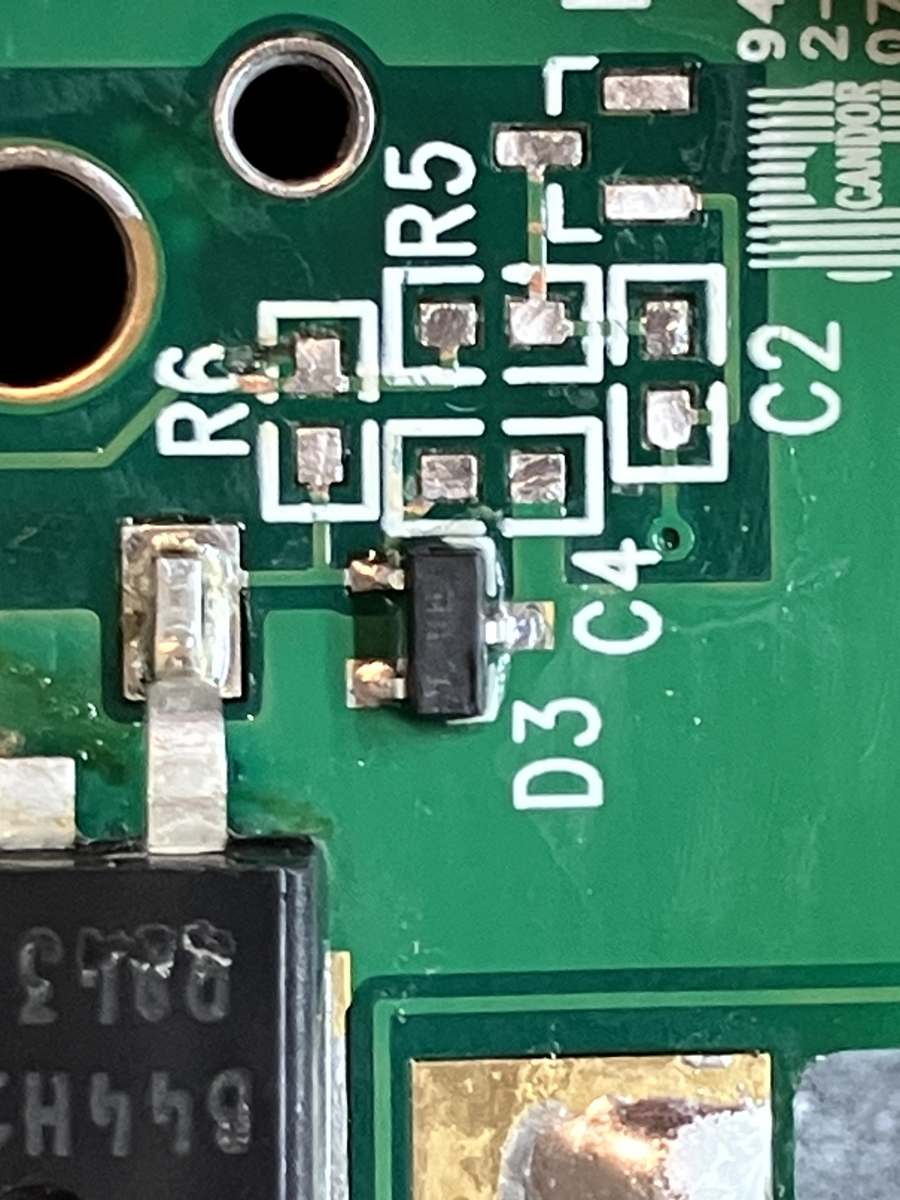
Q2 Complex
My best guess is D3 (probably a Zener diode acting as a voltage regulator) combined with R6 (which may be a precision resistor, based on it's package color) form some kind of stable current reference based on cell string output voltage.
This, in turn, through some analog magic I don't understand, switches on and off Q2, and thus the battery output. This doesn't explain why Q2 and Q1 are in parallel, however - if either one of them is closed, the output contacts are going to be energized.
Could Q2 be some kind of "emergency backup" for Q1/U1? A fail-over system in case U1 kicks the bucket for some reason? It also doesn't explain why Q2 is an NPN BJT and not another MOSFET. Why would they choose a completely different technology?
I could certainly see a backup circuit using a part from a different manufacturer, but a whole different type of transistor? My personal option is the Q2 complex is vestigial, an artifact of the manufacturing process. That is, these parts actually do nothing of use and are here because Harris didn't want to throw away a production run of parts, and/or didn't want to pay to rework a bunch of boards. Potential evidence of this is (a) a lot of the parts for the Q2 complex aren't place/installed, and (b) there are two poly-fuses in parallel. Wiring fuses in parallel is simply incorrect, from an electronics design stand-point.
Fuses don't act like resistors, they don't "share" current.
Minor differences in the fuse resistances due to manufacturing tolerances will cause one to sink more than it's "fair share" of current and then "pop", and the second fuse - now shouldering the entire load - will quickly follow along and open as well. The question then is, why are there two fuses? I suspect, by accident or design, these assemblies went part-way through the assembly process for the Q2 complex.
This included Q2 and P1, as well R6 and C4. For whatever reason, these partial assemblies were then redirected to another production line, and the full install for the Q1/U1 complex was performed, filling out the actual functional electronics. This resulted in both fuses being installed - which just happened to be identical parts. Installing another fuse would have been a waste of money, honestly, but maybe the production line for Q1/U1 was already set up and configured, pick and place machines loaded, so they just ran their stock of boards through. Very strange, all around.
Schematic
I took some time to draw out most of the PCB as a schematic diagram, click the image below to get the PDF. Note that this is best-effort, and is incomplete - this only covers parts and traces that appear to be populated/used, and I didn't chase down all the pins/traces on U1.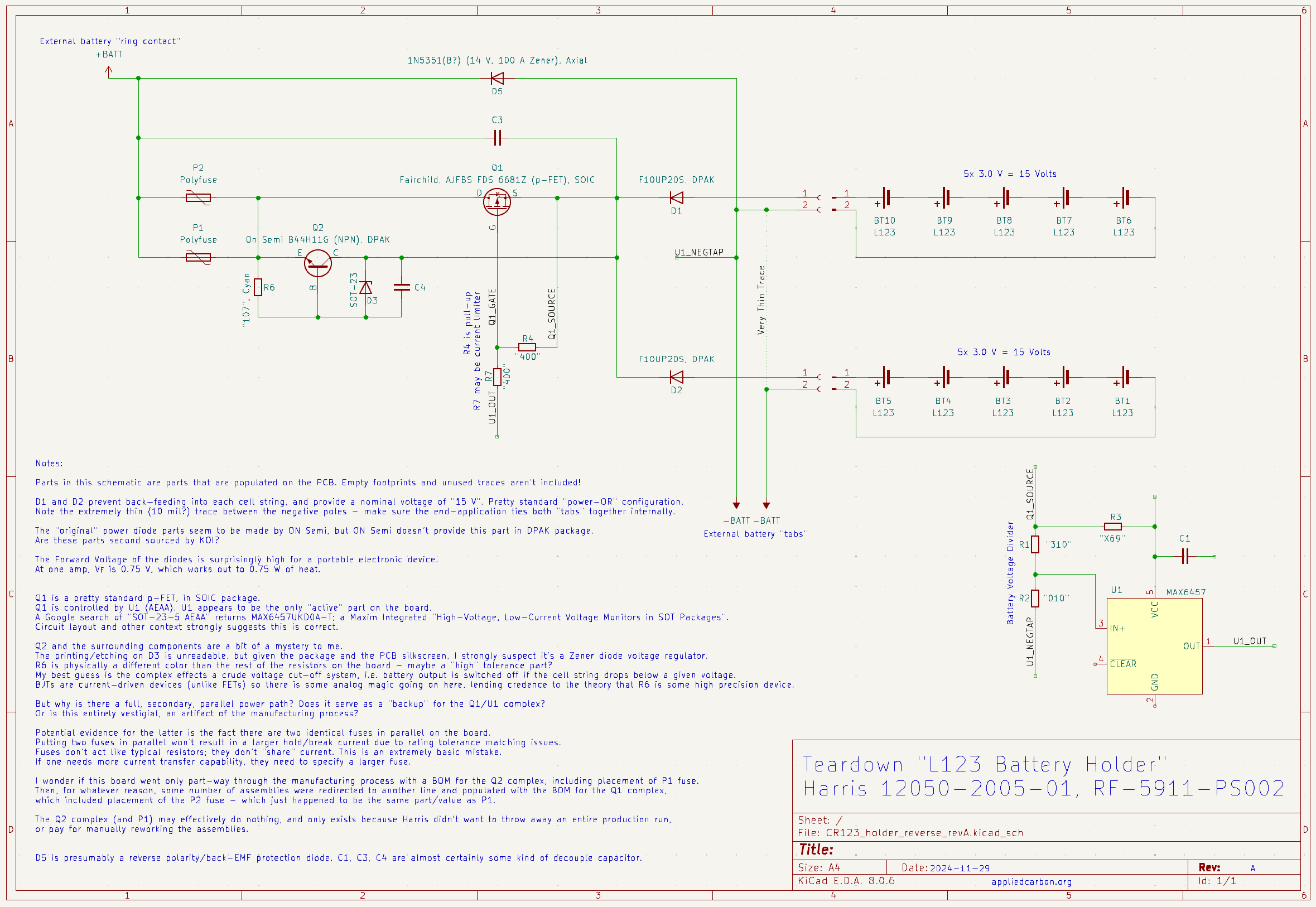
Click for PDF