
65C02 Single Board Computer
Last Update: September 29, 2014
- Introduction
- Features At a Glance
- Block Diagram
- Schematic Diagram
- Memory Map
- XPAN Connector
- Part List
- Firmware & Bootloader
- Appendix A: Complex Programmable Logic Device (CPLD)
- Appendix B: Using a network card to program the flash chip
Introduction
Note: This project is under development; this document is incomplete at this time and may be inconsistent. This project is actually the result of several ideas that managed to coalesce into a single project. Building a computer around one of the old 'classic' microprocessors (Z80, 6502, 8051, 68k) has been something I wanted to do for a while - call it nostalgia for a simpler time. It was also born out of frustration with 'simple' low cost development systems intended for students and beginner hobbyists, namely the Arduino and Raspberry Pi. These platforms are a good introductions to electronics but the all-in-one nature of the CPUs and the slick software development environments abstracts away almost all the complexities. While there is educational value in these systems, I've discovered that the end users tend to treat them as mysterious black boxes - people tend to rely on blobs of code and libraries that they only understand enough to know that if they feed it data X it will do Y. A chance conversation in a bar convinced me there was a market for a much more open and lower level learning tool. Modern microcontrollers and SoCs are complex devices with equally complex and opaque tool chains. My idea was to break open those chips (not literally) and lay out a simplified version of the internals for a user to poke and prod with multimeters, oscilloscopes and logic analyzers. This board is designed to be as simple as possible: a microprocessor, RAM, non-volatile storage, a serial port, an expansion bus, and some glue logic. All the parts are through-hole and easy to solder. Many of them are in DIP packages so the user can pull them out and use them on a solderless breadboard or their own boards. The parts are also inexpensive and mostly generic - it should be easy to source replacements if there are any 'learning experiences'. I wanted to avoid complex, high level languages (to avoid the learning curves and resulting abstraction) and if possible avoid complier chains and IDEs altogether. The idea was to get people down onto the bare metal, up close and personal with the registers, the address bus, and the program counter. It made sense to use an older microprocessor as these tend to be straightforward in terms of architecture and design. The 6502 is well characterized, there is plenty of documentation available, it's still in commercial production, and it's relatively simple to program (I've seen someone write industrial control software with nothing but a legal pad and a calculator). As a bonus, the kit has been designed to fit onto the Parallax Board Of Education Robot (BoE-bot) frame. This kit does not contain the hardware needed to operate the BoE-bot chassis, but I'm developing an ecosystem of boards to provide that functionality.Features At a Glance
- Designed around the Rockwell 65C02 microprocessor and equivalents
- 32k x 8 bit SRAM
- 32k x 8 bit flash non-volatile storage ("ROM")
- 16C550 UART (16 byte FIFO for both TX and RX, standard modem interface)
- Power On Reset (POR) monitor circuit
- Complex Programmable Logic Device (CPLD) (implements 'glue' logic)
- Expansion header (provides power, ground, data bus, address bus, clocks, and three memory mapped assert signals)
- On-board 5V power supply
- 3.050" x 4.000" four layer printed circuit board
- 0.25" mounting holes on 2.750" x 3.700" centers (compatible with Parallax BoE-bot chassis)
Block Diagram
Schematic Diagram
Schematic in EPS and PNG.
Bill of Materials
TODO!Memory Map
Note that the flash chip you receive may not be exactly 32KBytes in size; it will probably be larger. In fact, any flash chip larger than 32KBytes will work with the system (provided the pin-out of the parts are identical). As memory prices have dropped, the market for lower capacity storage devices has shrunk to the point where parts with excess space are actually cheaper than parts that are the 'correct' size.The kit, as shipped, cannot utilize the extra space on the flash chip.
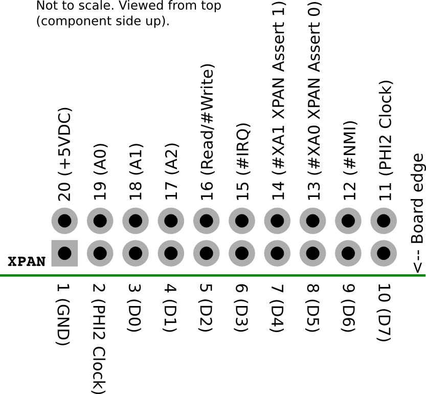
XPAN Connector
The XPAN (eXPANsion) connector was designed with the idea that extra boards could be stacked on top (or under) the primary board and 20-pin IDC connectors and a ribbon cable would be used to connect together all the boards in the stack. The XPAN connector provides access to the following signals:- +5VDC power
- Ground
- Eight bit data bus
- Address lines A0, A1, and A2
- Phi-2 clock signal
- Phi-1 clock signal
- Read/#Write signal
- Interrupt Request (#IRQ) signal
- Non-maskable Interrupt (#NMI) signal
- Two-bit memory mapped prehiprial assert signals
 Memory mapped prehiprial assert signals (XPAN Assert Signals) are active low, and their label number matches their bus value:
| Bus Value (#XA1, #XA0) | Memory Block Address Range (inclusive) | Description | ||
|---|---|---|---|---|
| 0 | 0 | 0x7FD0 | 0x7FD7 | XPAN Assert Signal 0 |
| 0 | 1 | 0x7FD8 | 0x7FDF | XPAN Assert Signal 1 |
| 1 | 0 | 0x7FE0 | 0x7FE7 | XPAN Assert Signal 2 |
| 1 | 1 | N/A | N/A | No prehiprial selected |
Firmware & Bootloader
Requiring the use of an external flash programmer would incur wear and tear to the board, raise the cost of the kit, and slow down development. Therefore the flash chip is attached so that the 65C02 reset vector is located in its top 4KByte sector. This sector contains a bootloader that checks for (and downloads) new flash memory images into SRAM. The bootloader first configures the UART and then watches for a handshake signal from an attached device. If it detects this signal the bootloader will download and write a user-provided binary blob to [to be determined spot] in SRAM. If no handshake is present (the software will wait about one second) the bootloader will leave the UART as is (thus preconfiguring it for the user) and then jump execution to [to be determined] on the bus ([to be determined] on the SRAM chip). The bootloader will not overwrite itself, nor will it change the contents of the flash chip. If you want to modify the bootloader or rewrite the contents of the entire chip for whatever reason you will need to remove the flash chip from the board and use an external programmer. You may be interested in the contents of Appendix B.Appendix A: Complex Programmable Logic Device (CPLD)
The use of a CPLD was a trade-off between sticking to the original design mandate of 'down to the metal', and having to fit all the parts needed to implement the glue logic onto a three inch by four inch board. Sadly it adds one of those 'black boxes' I was arguing against in the introduction (as well as requiring specialized IDEs, compilers, uploaders...). While detailed instruction on HDL development and CPLD programming is beyond the scope of this document I can provide some basic information to get a more advanced user started. As shipped, the CPLD in the kit comes preprogrammed with software to map various memory locations to the SRAM, flash, UART, and several pins on the XPAN connector, as well as handling some interrupt signals. The default firmware for the CPLD is available in both Verilog code and Serial Vector Format (.svf). If you do want to modify the CPLD firmware you will need to download Alteras CPLD/FPGA development software, Quartus II. A stripped-down free version is available although you may need to create an account. You will also need a appropriate JTAG cable/dongle and programming software that interprets the file generated by Quartus and programs the resulting bitstream into the CPLD. For the development of this project I used a clone of an Altera ByteBlaster parallel port cable and ran the Quartus software inside a virtual machine on my workstation. The CPLD is programmed and debuged via the Joint Task Action Group (JTAG) Test And Program (TAP) port. Most people just refer to these ports as 'JTAG sockets' or similar. On this board the TAP port is labeled 'JTAG' and is on the right hand side, near the edge. The pinout is identical to the standard Altera and Atmel AVR JTAG adapter cables: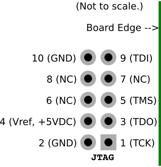
I also attempted to use UrJTAG along with a Xilinx DLC-5 cable but was unsuccessful. YMMV.
Appendix B: Using a network card to program a flash chip
If one wants to develop a custom bootloader or want to load custom code onto the board that (for example) makes direct use of the reset and interrupt vectors, one will need to program the flash chip outside the board. (The default bootloader cannot update or overwrite itself.) The price of professional programming rigs are easily in the three digit range, and these systems are overkill for the average hobbyist or student. At the opposite end of the spectrum are imported programmers that are relatively cheap but tend to be of questionable build quality and limited manufacturer support.Here is an alternate solution:
There is a nifty little Linux utility called flashrom (a spin-off project from the Coreboot project) that allows users to read/erase/write the contents of flash chips on mainboards, network/graphics/storage controller cards, and various other programmer devices. Most mainstream distributions will probably have it in their repositories. As luck would have it, a number of older network cards have a PLCC-32 socket on them for a flash or ROM chip, intended to hold firmware and data needed for booting a computer over a network connection. One can usually find these cards at swap meets or recyclers for a few dollars, if they don't already have a suitable card in a spare parts box somewhere. The flashrom supported hardware page is extensive. I personally used a SMC 1211TX Ethernet network card which falls under the nicrealtek driver on a system running Fedora 20: WARNING: Modifying the contents of the wrong chip may render your computer non-functional! Verify the chip part number and card PCI address!
Values used below are for example purposes only, your commands may vary!
	[root@localhost ~]# flashrom -p nicrealtek:pci=00:0a.0
	flashrom v0.9.6.1-r1705 on Linux 3.12.6-300.fc20.i686+PAE (i686)
	flashrom is free software, get the source code at http://www.flashrom.org

	Calibrating delay loop... OK.
	Found SST flash chip "SST39SF010A" (128 kB, Parallel) on nicrealtek.
	No operations were specified.


	[root@localhost ~]# flashrom -p nicrealtek:pci=00:0a.0 -r backup_flash.rom


	[root@localhost ~]# flashrom -p nicrealtek:pci=00:0a.0 -w new_flash.rom
It is important to note that the interface for many parallel interface flash chips are identical; just because a given chip is not on the list does not mean flashrom can't be forced to program it.